
Technology
|
|
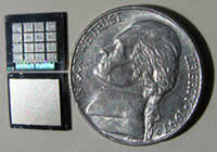
Packaged Nanochip storage system bottom left |
||
|
MEMS Nanochip’s core technology is array atomic probes, moved
with Micro-Electrical Mechanical System (‘MEMS’) actuators,
combined with ultra-dense, nonvolatile, re-writable media. The process
of fabrication is entirely performed by semiconductor fabrication
tools in mass production, utilizing silicon wafer substrates. Two
wafers containing the "head stack" die on one wafer, and
the media on another wafer, are bonded together. This wafer stack
is sawed into individual die pairs to form the storage units. Each
die pair contains the read/write heads on one die and the other
the data storage media. Bit densities of 1 Terabit/in2
are typical. The storage substrate utilizes a proprietary technology,
with demonstrated rewrite cycles exceeding 1013. |
|||
|
Atomic Probes
|
|||
 Nanochip's
core technology is high-capacity memory devices built with semiconductor
fabrication tools. Nanochips manipulate data on a molecular scale
to allow ultra high-density storage.
Nanochip's
core technology is high-capacity memory devices built with semiconductor
fabrication tools. Nanochips manipulate data on a molecular scale
to allow ultra high-density storage.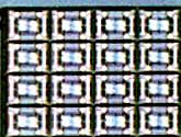
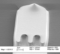 Nanochips
utilize atomic scale probes of a unique design to interact with
the media. These atomic probes enable Nanochips to read and write
at ultra high densities exceeding 1 Terabit/in2.
Nanochips
utilize atomic scale probes of a unique design to interact with
the media. These atomic probes enable Nanochips to read and write
at ultra high densities exceeding 1 Terabit/in2.